
Semiconductor Industry Parts CNC Machining
Semiconductor FAQs
What you may want to know about Semiconductor
Semiconductor Parts CNC Machining Service's Features & Targeted Applications
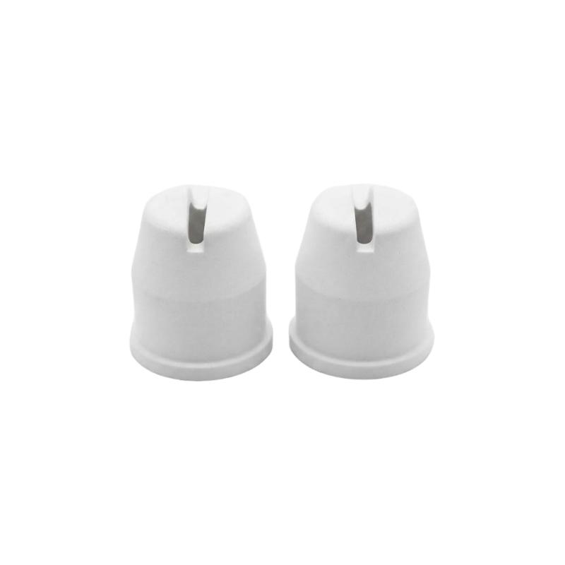
FlexiTurn's Semiconductor Parts CNC Machining services offer sub-micron tolerance control, ultra-low outgassing rates, and excellent surface defect control, specifically engineered for high-vacuum, high-purity, and severely corrosive non-standard semiconductor components. Our custom parts are widely used in front-end wafer fabrication equipment (thin-film deposition CVD/PVD, plasma etching, lithography, ion implantation, chemical mechanical planarization CMP) and back-end packaging/testing equipment (die attach, dicing, IC handlers).
By optimizing cutting paths, tool selection, and ultra-precision polishing processes, these components maintain zero outgassing, zero particulate contamination, and absolute dimensional stability under ultra-high vacuum (UHV down to 10-9 Torr), intense plasma bombardment, high-frequency thermal cycling, and aggressive acid/alkali chemical cleaning. In chip manufacturing where yield and zero downtime are critical, FlexiTurn cnc machining services are trusted by global semiconductor equipment clients.
Semiconductor Parts CNC Machining Service's Materials, Vacuum & Plasma-Resistant Design
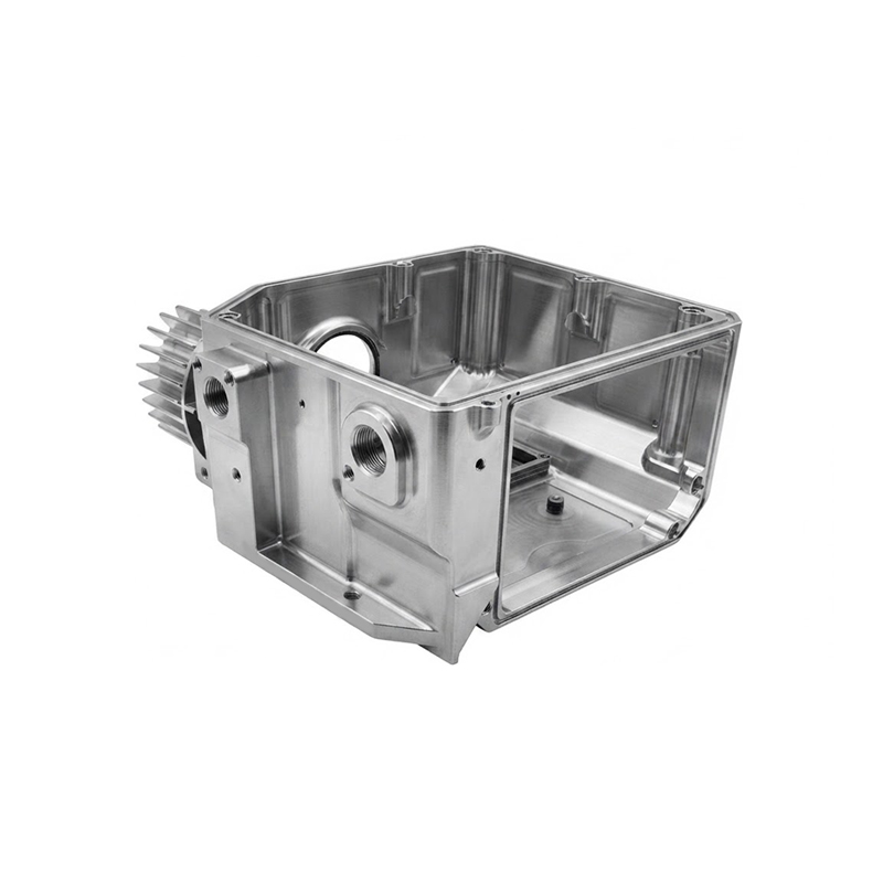
Preventing vacuum leaks, eliminating dead spaces that trap gases, and resisting plasma erosion are core mechanical design goals in semiconductor engineering. During initial Design for Manufacturing (DFM) reviews, our engineering team evaluates your CAD drawings to optimize flow channel angles, eliminate stagnant zones, check geometric tolerances on micro-O-ring grooves, and utilize monolithic (one-piece) 5-axis CNC machining to replace multi-part assemblies—reducing leakage risks and boosting vacuum sealing reliability.
To satisfy different process demands (such as high-temperature annealing or low-temperature acid etching) regarding dielectric constants, high thermal conductivity, hardness, or wear resistance, we offer fully customizable material and surface treatment options tailored to your specific equipment conditions (such as plasma power and gas composition). FlexiTurn maintains a complete semiconductor-grade raw material matrix:
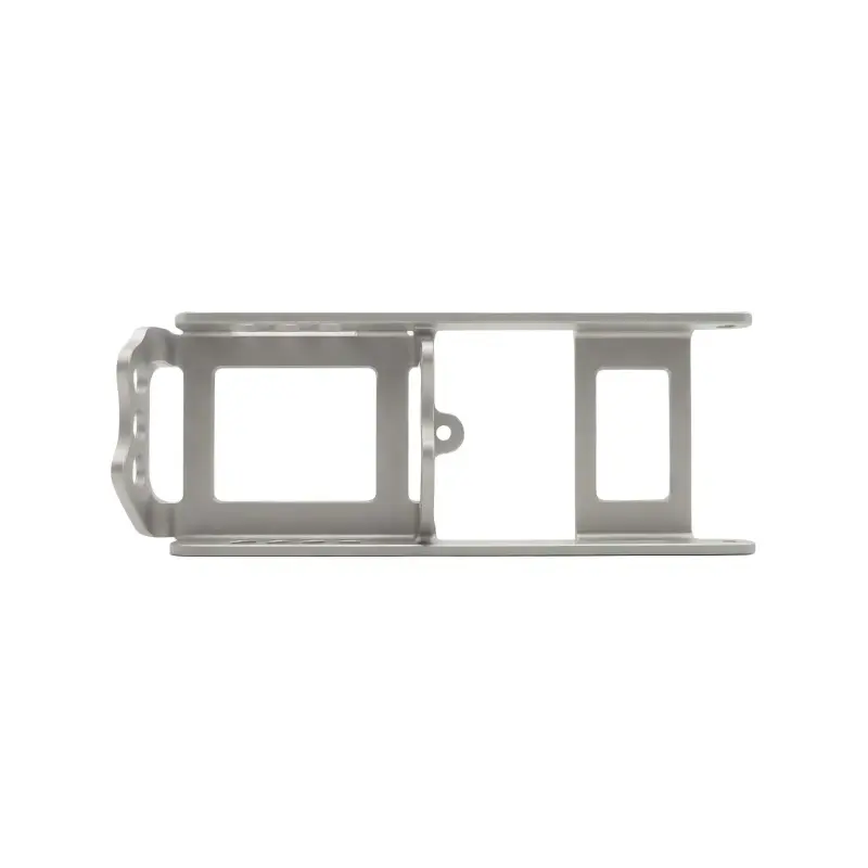
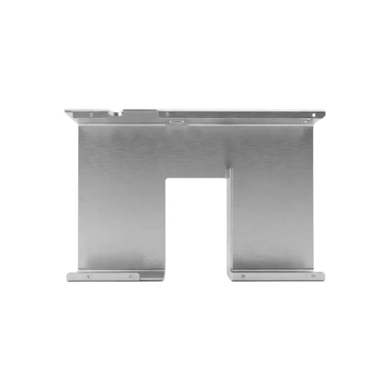
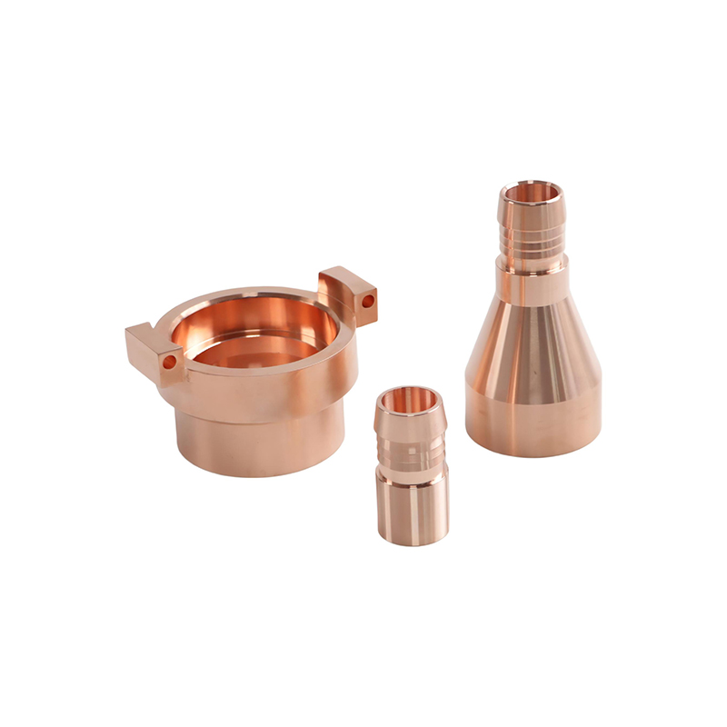
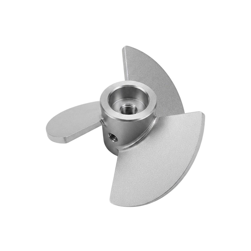
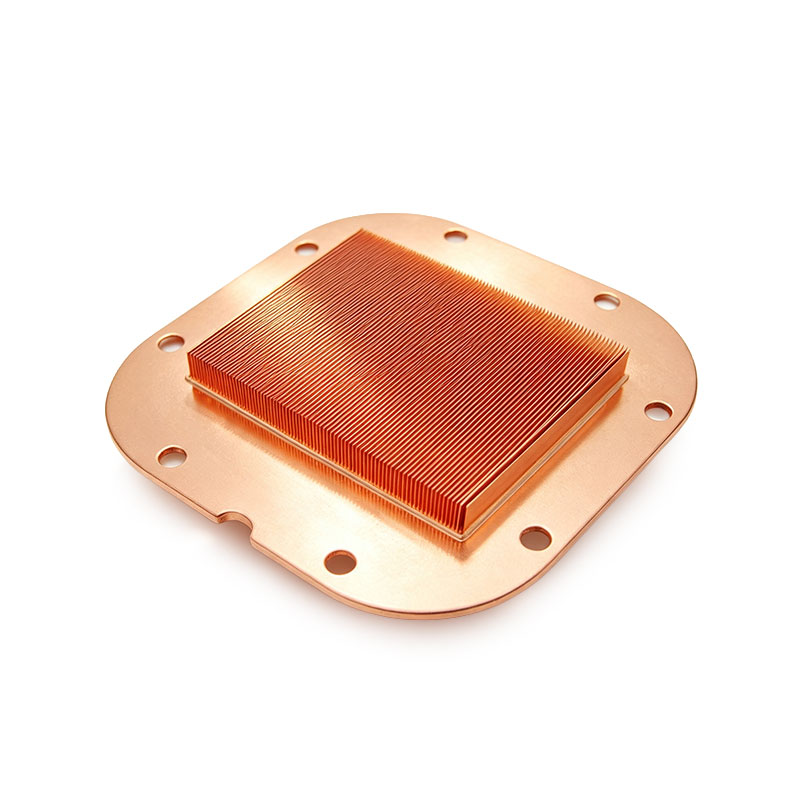
Semiconductor Metals: 6061-T6/7075-T6 aluminum alloys, 316L VIM/VAR stainless steel, High-Purity Oxygen-Free Copper (OFHC), Inconel nickel-based alloys, Titanium alloys, etc.
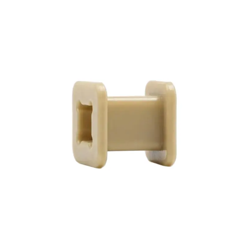
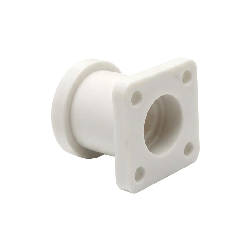
Polymers & Engineering Plastics: PTFE (Teflon), PEEK, POM, VESPEL (high-grade polyimide), etc.
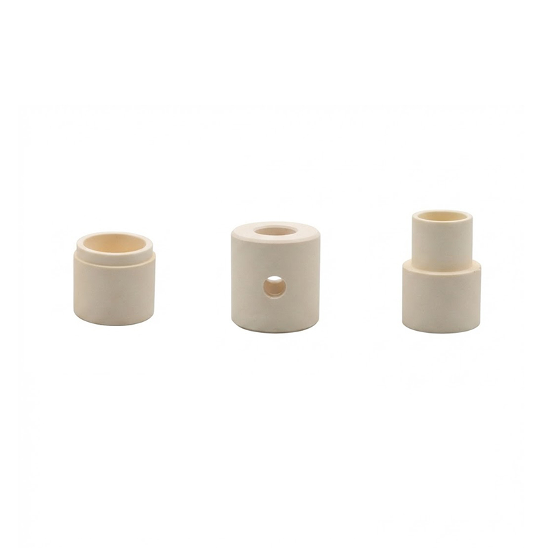
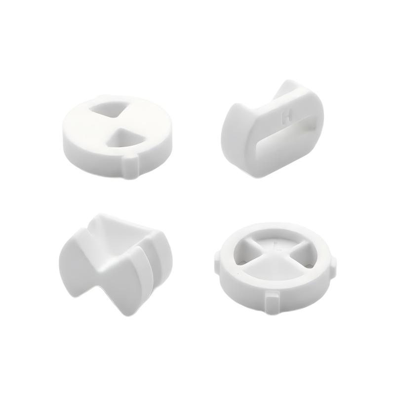
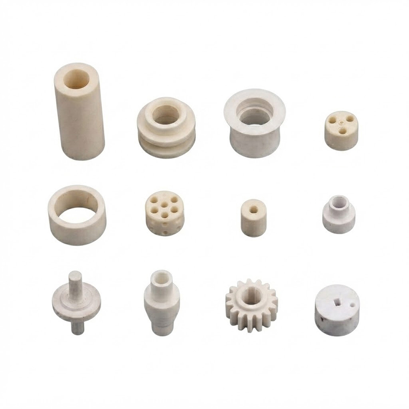
Inorganic & Specialty Materials: Quartz, high-purity single-crystal/polycrystalline Silicon, Alumina/Aluminum Nitride precision ceramics, etc.
Semiconductor Parts CNC Machining Service's Core Machining Operations for Semiconductor Parts
Depending on geometry, micro-hole distribution, and ultra-high tolerance requirements, FlexiTurn offers precise, cost-effective CNC processes:
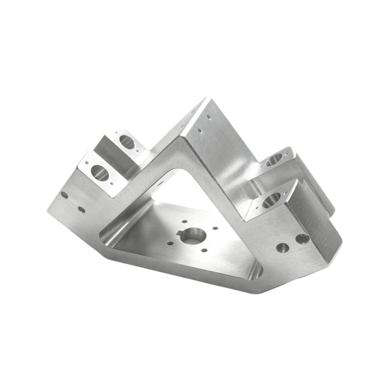
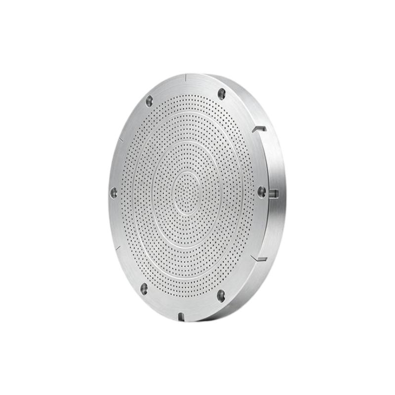
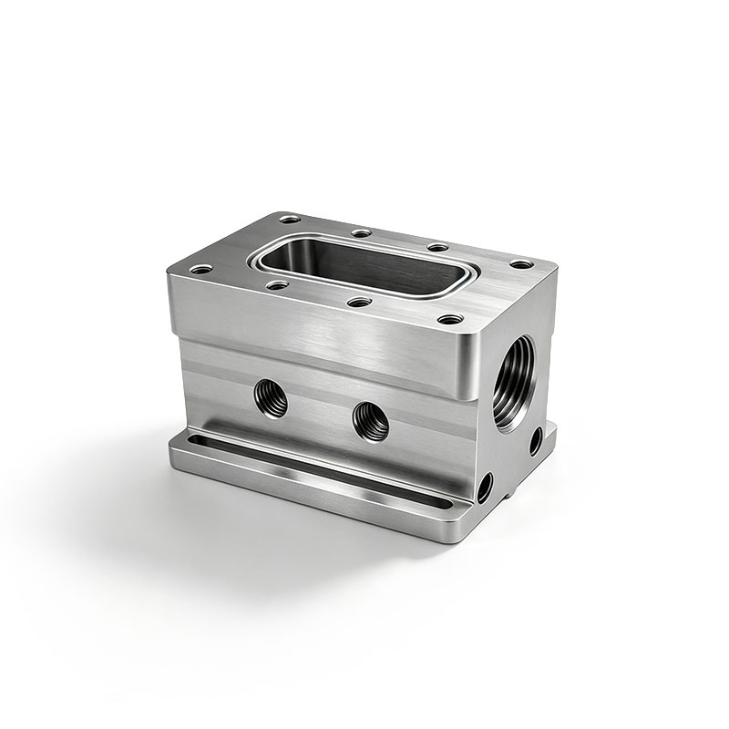
5-Axis CNC Milling: Ideal for complex etch reaction chambers, CVD gas distribution showerheads, multi-channel fluid manifold blocks, and lithography positioning stages.
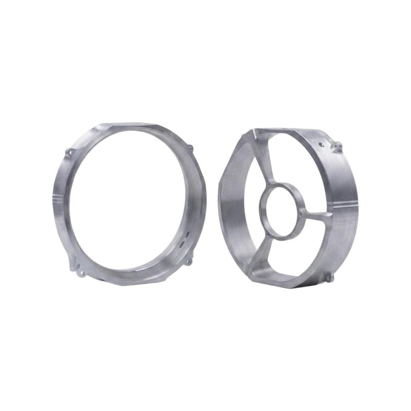
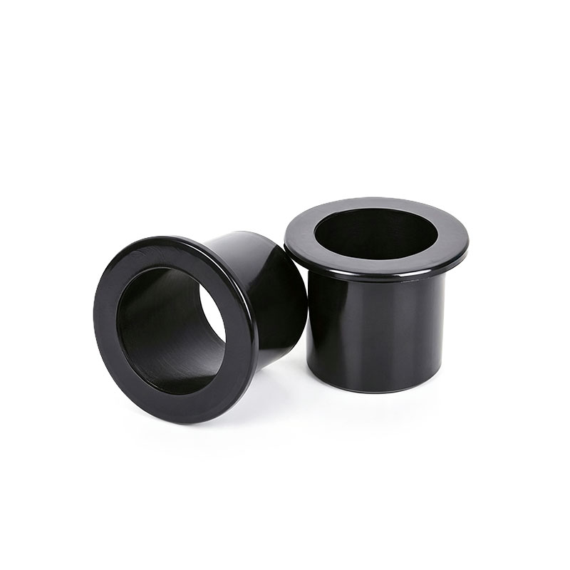
Precision Turning & Mirror Facing: Used for cylindrical chambers, wafer carrier rings, RF matcher interfaces, and high-vacuum flanges (CF/KF/ISO flanges) requiring high concentricity.
Micro-Drilling & High-Density Array Drilling: Cuts thousands of burr-free micro-holes in aluminum alloys or ceramics for gas showerheads and cleaning equipment distribution plates, ensuring uniform gas/liquid injection.
High-Precision Sealing Groove Cutting: Cuts knife-edge flanges (CF flanges), rectangular sealing grooves, and micro-O-ring grooves for vacuum sealing, holding tolerances within microns for leak-tight performance.
Semiconductor Parts CNC Machining Service's Integrated Post-Processes & Cleanroom Finishes
Beyond core turning and milling, FlexiTurn integrates secondary manufacturing capabilities to deliver ready-to-assemble hardware for cleanroom environments:
Secondary Processing & Precision Polishing: Mirror polishing (achieving ultra-low roughness), chemical mechanical polishing (CMP), laser engraving (micro QR codes/serial numbers), and deep-hole drilling.
Semiconductor Finishes: Semiconductor-grade hard anodizing, electropolishing (EP, significantly reducing surface absorption and outgassing), electroless nickel plating (ENP), gold/silver plating, and fluororesin coatings for extreme corrosion resistance and low contamination.
Ultra-Clean Cleaning & Packaging: Multi-stage ultrasonic DI water cleaning, baking, and double-layer anti-static vacuum bag packaging inside a cleanroom.
Semiconductor Parts CNC Machining Service's Advanced Customizable Engineering Support
At FlexiTurn, everything is fully customizable. We don't just follow drawings; we recommend optimal material and surface treatment combinations based on how your parts experience stress, temperature, and chemical media in real-world operation. We provide complete engineering support—from single-piece rapid prototyping and low-volume pilot runs (down to dozens of units) to full mass production—helping semiconductor equipment companies shorten R&D cycles and reduce operational risks.
Contact Our Semiconductor Technical Team
Ready to start your semiconductor component project? Send your CAD drawings (.STP/.IGS/.DXF) and specific cleanliness/tolerance requirements to our engineering team at sales@flexiturn.com. Our senior engineers will deliver a comprehensive DFM report and a competitive factory-direct quote within 24 hours.